How Intel is Using ASML’s High NA EUV Technology
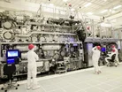
Intel has become the first manufacturer to use ASML’s High NA EUV technology in mass-produced chips.
The technology company has begun high-volume manufacturing for the Core Ultra Series 3 processors at its site in Hillsboro, Oregon, US.
Specific Intel 18A layers are now dual-qualified on High NA EUV in Oregon, US proving as capable to match the same yield as the NXE machines.
This is set to make Intel the first company to make use of High NA EUV technology in mass production.
Naga Chandrasekaran, Executive Vice President and General Manager of Intel Foundry, says: “This milestone reflects the close technical collaboration between Intel and ASML and shows how High NA EUV can be integrated into advanced semiconductor manufacturing at scale.”
Production with High NA EUV technology
Code named Panther Lake, Intel’s Core Ultra Series 3 processors are built on Intel 18A, and only certain layers will be built with High NA EUV technology.
The chip is used in Intel’s next generation mobile and laptop software, rather than on desktop.
In January 2026, Intel announced that its new processor will be launched with 14 chips across five products and used in more than 200 PC setups.
Intel's site in Oregon is primarily used during the initial creation and foundation stage of its chip manufacturing.
The processors are then transferred to other factories around the world for full production.
Intel will be the first company to implement High NA EUV technology in mass production, doing so before TSMC.

Intel’s 14A process node
Intel’s relationship with ASML dates back to 2012, but the technology company did not receive its first High NA EUV machine until January 2024.
After combining to produce the first commercial chip that uses High NA EUV lithography, Intel and ASML are already planning new concepts.
In 2027, Intel is set to begin risk production for its 14A process node that will be fully constructed by ASML’s High NA EUV system for the first time.
Mass production is not expected until 2028 and in April 2026, Elon Musk revealed that Tesla’s Terafab plant will use the technology in its chips.
Christophe Fouquet, ASML's President and CEO, says: “With increased resolution and better process control, the introduction of High NA EUV marks a substantial development in semiconductor lithography.
“We are proud to play a role in enabling the smaller, denser patterning that will accelerate advancements in AI and other emerging technologies.”
Company portals


Executives
Christophe Fouquet
President and Chief Executive Officer

Naga Chandrasekaran
Chief Technology and Operations Officer, EVP & GM of Intel Foundry Technology and Manufacturing