Sony & TSMC's Plans to Manufacture Physical AI Image Sensors

Sony Semiconductor Solutions and TSMC have signed a memorandum of understanding to set up new production lines in Sony’s Fab in Koshi City, Japan for the development of “next-generation” image sensors.
As part of the partnership, the companies intend to explore opportunities in physical AI applications in automotive and robotics industries.
The companies have previously partnered on TSMC’s chip plant in Japan.

Sony's agreement with TSMC
Sony and TSMC intend to establish a joint venture to set up development and production lines for image sensors in Sony’s newly constructed fab in Koshi City, Kumamoto Prefecture, Japan.
The companies are discussing potential investments under the joint venture. In a press release, the companies say that the investments, along with new capital investment by Sony in its existing plant in Nagasaki, are being considered on the premise that they would be implemented in phases.
These phases are based on market demand and support from the Japanese government.
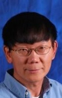
TSMC Senior Vice President and Deputy Co-COO, Dr. Kevin Zhang, says: “Sony has been our long-time partner in the CMOS image sensor business. We are excited to elevate our collaboration to the next level, which represents a key step forward in driving future sensing technology in the AI era.
“This partnership underscores our shared commitment and mutual vision of leveraging cutting-edge technologies and innovative solutions to deliver leading sensing technology and products.
"We look forward to working closely together to achieve impactful results and create lasting value for all stakeholders.”
Image sensors for automotives and EVs
Sony Semiconductor Solutions has the largest share of the image sensor market. Its products are used in industrial applications, consumer cameras, automotives and mobile phones.
McKinsey said March 2026 that the overall sensor market could reach US$45bn by 2035 and the LiDAR sensor market is poised for exceptional growth.
This comes as advanced driver assistance systems and autonomous driving adoption accelerates, while demand for traditional powertrain sensors slowly decreases with the rise of electric vehicles.
On its website, Sony says that its Automotive cameras, or LiDAR, function as “eyes of vehicles” for enabling automotive systems to monitor the peripheral conditions and grasp the presence of obstacles. They can be used in Advanced Driver Assistance Programs and have applications in automated driving systems.
Physical AI and technological developments
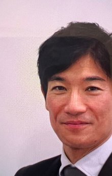
Shinji Sashida, CEO of Sony Semiconductor Solutions, says “This joint venture is a significant initiative that brings together the strengths of both companies and aims to drive further advancement in technology and business within the next-generation image sensor field.”
The companies say that the partnership also seeks to explore and address emerging opportunities in physical AI applications, such as automotive and robotics.
In a press release the companies argue the collaboration is “paving the way” for “future innovations” and “expanded technological advancements”. The press release noted that under the proposed partnership Sony would function as the majority and controlling shareholder.
Shinji says: “Building on the trust cultivated through our long-standing collaboration with TSMC, I am delighted that we have reached an agreement to advance our partnership to a new stage.
“Building on this joint venture, Sony intends to further strengthen its business operations with a focus on creating high added value. Rooted in the Sony Spirit that has guided us since our founding, we intend to continue to take on the challenge of creating new markets through unprecedented ideas and distinctive technologies.”
Company portals


Executives
Kevin Zhang
Deputy Co-COO and SVP
Shinji Sashida
Executive Vice President Senior GM