NVIDIA AI is Accelerating TSMC's Semiconductor Manufacturing
NVIDIA has announced that TSMC is using its accelerated computing and AI to advance semiconductor design and manufacturing.
It says this helps to improve turnaround time, energy efficiency, yield and operational productivity in fabs.
Global semiconductor demand is skyrocketing, driven primarily by an need for AI infrastructure, data centres and advanced memory.
“TSMC and NVIDIA have built a long-standing partnership rooted in advancing the technologies that make the next generation of computing possible,” says Dr. C.C. Wei, Chairman and CEO of TSMC.
“By using NVIDIA accelerated computing and AI across fab operations optimisation, lithography, process control and inspection, TSMC is strengthening our technology leadership and manufacturing excellence to support our customers’ future products and success.”
NVIDIA CUDA-X
CUDA-X libraries and AI models are being put to work on NVIDIA GPUs for a variety of processes.
For computational lithography, TSMC is using NVIDIA cuLitho that delivers a 20 to 50% improvement in cost effectiveness or cycle time compared with CPU-based computational lithography.
cuEST is another part of TSMC's toolkit, a GPU-accelerated electronic structure simulation library.
NVIDIA says this can deliver on average 50 times faster chemistry simulations for material design.
For advanced process control, cuML is used to accelerate large-scale analytics.
GPU-accelerated scheduling computation using CUDA has also brought TSMC "notable improvements" in fab productivity, NVIDIA says.

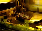
Semiconductor defect inspection
Since advanced nodes can cost up to US$20,000 per wafer, even a minor defect can translate to millions in losses.
Defects on a nanometre scale can cause an entire wafer to be unusable.
NVIDIA's Metropolis and TAO Toolkit are also used to improve defect classification inside fabs.
The company says these capabilities help TSMC to improve quality inspection and reduce the need for repeated labelling and retraining.
Digital twins for advanced fabs
Advanced semiconductor fabs are some of the most complex factories, with precise coordination required across humans, robots, tools, materials and building systems.
NVIDIA says TSMC is looking to its Omniverse libraries to build FabTwin, a digital twin fab environment.
This would support evaluating process tool layouts and related simulation workflows, allowing for identification of potential configuration constraints early.
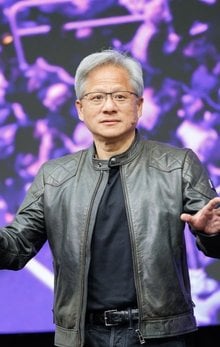
“NVIDIA and TSMC have worked together for nearly three decades to push the limits of computing,” says Jensen Huang, Founder and CEO of NVIDIA.
“TSMC is bringing NVIDIA AI and accelerated computing into the fab itself, tackling some of the world’s most complex design and manufacturing challenges with simulation, optimisation and AI to improve speed, efficiency and yield for the next generation of chips.”
Semiconductor demand
In May, the Semiconductor Industry Association (SIA) announced semiconductor sales in the first quarter of 2026 reached US$298.5bn, a 25% increase compared to the fourth quarter of 2025.
John Neuffer, SIA president and CEO, says: “Global chip sales remain on track to reach US$1 trillion in 2026.
“Strong sales across the Asia Pacific region, the Americas and China drove global semiconductor market growth, highlighting broad and robust demand for semiconductors and the countless tech products they enable.”
While there are thousands of semiconductor companies globally, only about 30 to 40 major corporations own and operate actual semiconductor fabs.
TSMC is the largest pure-play foundry, making chips for companies like Apple, NVIDIA and AMD.
Company portals


Executives

C. C. Wei
CEO
Jensen Huang
Founder and CEO